
|

|

|

|

|

|
The data acquisition system can be divided into 3 main parts: the audio transducers, the acquisition card and the acquisition software. Let's examine each of them in details.
Audio transducers
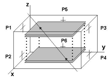
The first part of the data acquisition system is located inside the chamber. These 6 audio transducers collect the data coming from the spark. They are located as shown in figure beside. We need 3 of them at each point of the trajectory we want to determi ne. Since we make the assumption that their trajectory is a straight line, we take the beginning and the end points. With 3 reference points in space, we can determine the exact location without ambiguity of the very spot by which the particle travelled.
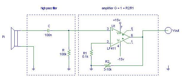
Each transducer has an amplification module associated with it in order to get a signal that is big enough to be considered by the acquisition card. These modules are glued to the exterior of the chamber and are connected to the transducers. The gain of t hese amplifiers is controlled by the trim resistor R2. We set the gain to 50 with a resistance value of 5 kΩ. Figure beside shows a scheme of an amplification module.
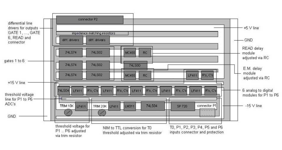
Figure 1 : Physical organisation of the acquisition card
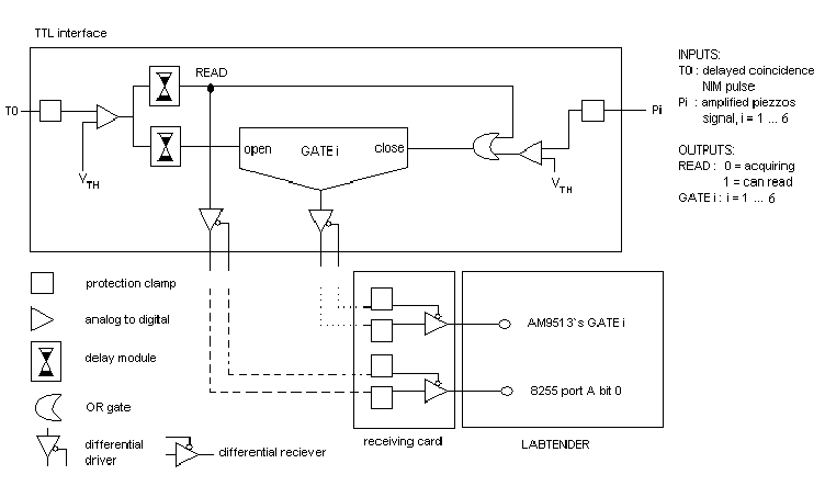
Figure 2 : Schematic view of the acquisition card
Secondly, we have to convert these signals into relevant inputs for the Lab Tender card. The acquisition card is itself divided into 3 parts: analog to TTL converters, delay units and differential drivers.
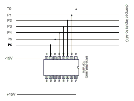 First, there are 7 converters on the card: a NIM to TTL converter for the coincidence pulse, called T0, and 6 analog to TTL converters for the 6 signals from the audio transducers, called P1 to P6. The inputs of all these modules are coming from a protection chip, SP720 from Harris Semiconductors, to prevent damag e to the IC's due to the electromagnetic pick-up caused by the chamber. The details of the connections are shown in figure beside. Figures 3 & 4 show the details of the connections for the converters.
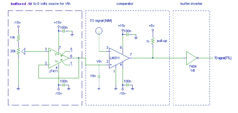
Figure 3 : NIM to TTL converter
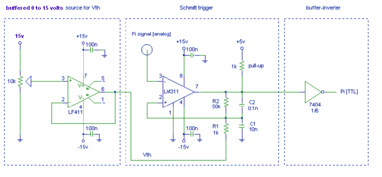
Figure 4 : Piezzo to TTL converter
The TTL signals are then used by the other chips of the card to generate the gate signals. The goal is to create digital pulses that will drive the Lab Tender. The logic is not so complicated but it will be described in great details in order for everyone to understand it.
The first signal to be processed is the T0 signal. It is first inverted using the 74LS00 from Texas Instruments and then sent to the timing chip MC1455 from Motorola as shown in figure 5. The timing chip basically takes a pulse and extends it to the width determined by the resistor and the capacitor of the timing setting part of the circuit. The time constant is then 1.1*RC. Ther e are 2 delay units. The output of the first is extended by a time constant of 24.1 microseconds (μs) and the output of the second is extended by a time constant of 4.76 milliseconds (ms). These values are determined by experimental data. The first s ignal is called ΔT and the complement of the second is called READ.
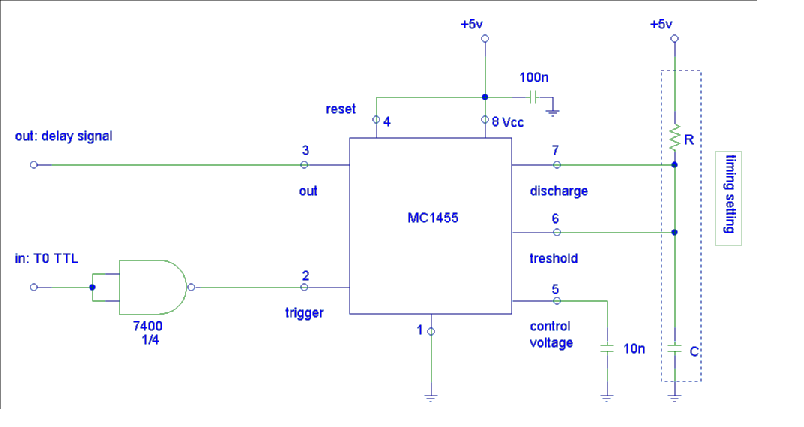
Figure 5 : Delay units
These signals are used as inputs for the 74LS74 from Texas Instruments, which is a gate generator. The gates are D edge-triggered flip-flops. The complement of ΔT is the clock input. The READ signal is NOR gated with each Pi[TTL] signal and the output of the NOR gate is the CLR input of the flip-flop. This is done to ensure that the gates will be closed even if there is no sound wave produced. The output Q of the flip-flop is ca lled the GATEi signal. There are ready to be used by the Lab Tender to enable the counters.
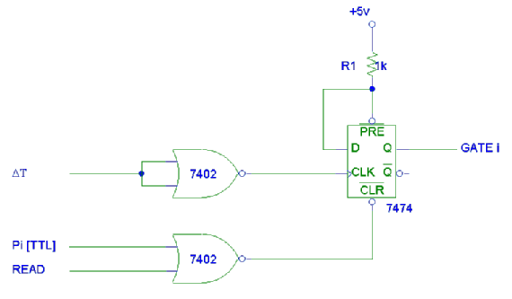
Figure 6 : Flip-Flops
The GATEi and T0 signals are then sent to the PC via twisted flat cables using differential drivers. A differential driver is a chip which outputs a signal and its complement. Using differential receivers, we can recover the original signal by substracting the complement to the signal. We can then eliminate the noise that could have been induced in the cables during the travel from the acquisition car d to the PC. Also, an impedance matching resistor of 120 Ω is placed between the outputs to avoid reflections in the cables. Inside the PC, a receiving card is placed before the Lab Tender. This card contains a protection circuit SP720 and the 6 differential receivers. There is also 2 outputs connectors that send the GATEi and the READ signals to the appropriate Lab Tender. This card is powered by the PC power supply.
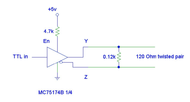
Figure 7 : Differential drivers
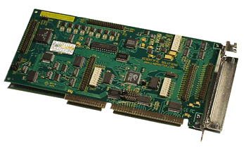
The acquisition software basically controls the Lab Tender card. It sends programming bytes to do basic operations on the different chips of the card and takes the data from these modules in order to save them in data files. Since there is only 5 counters on each card, we need 2 cards to process 6 input signals. Then, each operation of the program has to be done twice, as you can notice in the source code.
The Lab Tender card contains an analog to digital converter, a digital to analog converter, 5 16-bit counters and 5 parallel ports. For the purpose of this experiment, we only need the parall el ports and the counters. The counters basically count from the time they are open until they are closed and the parallel ports take the input signals to the gate of the counters. The times are given in an unknown unit. Since we are dealing with ratios of times and distances in our computations, we don't need to know it.

